China University of Technology breaks through the technical barrier of "difficult growth" of perovskite single crystal chips
Chinese scientists develop a new universal crystal growth technology.
Recently, I learned from East China University of Science and Technology that the school's clean energy materials and device team has independently developed a universal growth technology for perovskite monocrystalline wafers, shortening the crystal growth cycle from 7 days to 1.5 days, and realizing more than 30 kinds of metal halide The low-temperature, rapid and controllable preparation of perovskite semiconductors provides a rich material library for a new generation of high-performance optoelectronic devices. Relevant results were published in the international academic journal Nature Newsletter.
Metal halide perovskites are a new type of semiconductor materials with excellent optoelectronic properties and solution-ready. They have shown application prospects in the manufacturing of solar cells, light emitting diodes, radiation detectors and other devices. However, these devices currently mainly use perovskite polycrystalline films as photoactive materials, and their inherent defects can significantly reduce device performance and service life. If a perovskite monocrystalline wafer with a defect density of only one hundred thousandth of a polycrystalline film and excellent transport capacity and stability is used, higher-performance optoelectronic devices can be manufactured. Scientists compare polycrystalline thin films and monocrystalline slices to "broken diamonds" and "perfect diamond stones" respectively to show the advantages and disadvantages of the two.
▲ Researchers from East China University of Science and Technology demonstrated universal growth technology for perovskite monocrystalline wafers. Photo by Xinhua Agency reporter Wu Zhendong
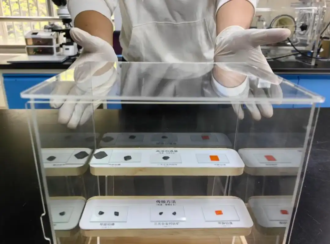
For a long time, there has been no general preparation method for perovskite monocrystalline wafers in the world. Traditional methods can only prepare several millimeter-sized single crystals in a way that meets the high temperature environment and slow growth rate, which greatly limits the practical application of monocrystalline wafers. Regarding the multiple processes involved in the growth of perovskite monocrystalline wafers, such as nucleation, dissolution, mass transfer, and reaction, the team of East China University of Science and Technology combined multiple experimental demonstrations and theoretical simulations to reveal that the mass transfer process is the key factor in determining the crystal growth rate. As a result, a growth system represented by dimethoxyethanol was developed, and the kinetic process of micelles was finely controlled by multiple coordinating groups, which increased the diffusion coefficient of solute by three times. In the high solute flux system, the researchers achieved a reduction in the temperature of the crystal growth environment by 60 degrees Celsius, a four-fold increase in the crystal growth rate, and a reduction in the growth cycle from 7 days to 1.5 days.
Hou Yu, a professor at East China University of Science and Technology and one of the main completers of this achievement, gave an example that at 70 degrees Celsius, the growth rate of methylamine lead iodine single crystal wafers can reach 8 microns/minute, and the size of the wafer can reach 2 centimeters in a crystallization cycle., which is a significant improvement from 4 millimeters under traditional methods. "We have broken through the technical barrier of insufficient solute diffusion in traditional growth systems and provided a more universal, more efficient and lower-condition monocrystalline wafer growth route."
Based on this breakthrough, the team assembled a high-performance single crystal wafer radiation detection device, which not only can realize self-powered radiation imaging and avoid the limitation of high working voltage, but also greatly reduce the radiation intensity. Taking chest X-ray imaging as an example, the new device The radiation intensity value is only 1% of that of conventional medical diagnosis.
